Skip to content
BEAM · MASKLESS LITHOGRAPHY

Desktop masklesslithography.

Sized for the lab bench, built for serious patterning.
<0.4 µm resolution · seamless stitching

NANYTE BEAM desktop maskless lithography system
RESULTS · IN THE WILD

Patterned with BEAM.

Real samples, real labs.

Dry-film resist on copper — patterned on the NANYTE BEAM maskless lithography system
01 / 08
Dry-film resist on copper
Cu / DFR · Single-layer exposure
Tapered nanowire bridges — patterned on the NANYTE BEAM maskless lithography system
02 / 08
Tapered nanowire bridges
AZ5214E · Single-layer exposure
Interdigitated capacitors — patterned on the NANYTE BEAM maskless lithography system
03 / 08
Interdigitated capacitors
AZ5214E · Single-layer exposure
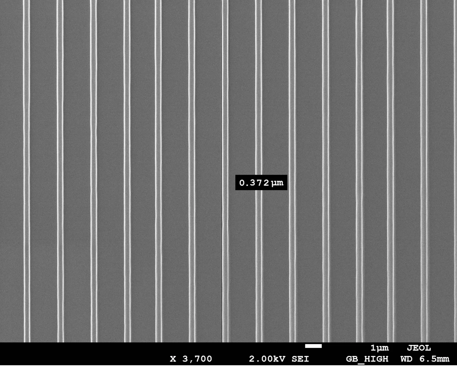
Cr nanowires after lift-off · SEM — patterned on the NANYTE BEAM maskless lithography system
04 / 08
Cr nanowires after lift-off · SEM
Cr / Si · Lift-off, positive resist
2 µm pillars in HSQ — patterned on the NANYTE BEAM maskless lithography system
05 / 08
2 µm pillars in HSQ
HSQ25 · Negative-tone exposure
Asymmetric split ring resonators — patterned on the NANYTE BEAM maskless lithography system
06 / 08
Asymmetric split ring resonators
Metallized resist · Single-layer · metallized
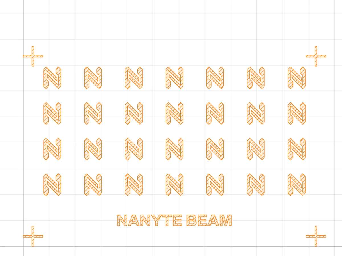
Stitched grid over many writefields — patterned on the NANYTE BEAM maskless lithography system
07 / 08
Stitched grid over many writefields
ECI3007, 700 nm · 1 µm lines · stitched
Lion head · greyscale relief — patterned on the NANYTE BEAM maskless lithography system
08 / 08
Lion head · greyscale relief
HSQ 20 µm · Greyscale exposure
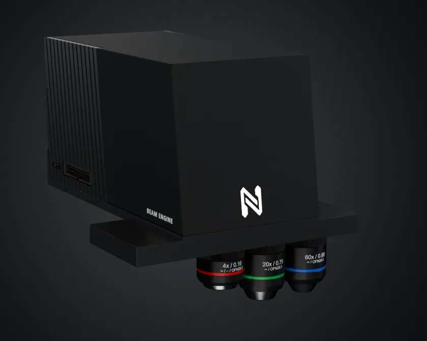
NANYTE BEAM Gen 2 optics engine — the swappable DMD direct-write module, product render
BEAM ENGINE · MODULAR
MODULAR DESIGN

One engine, built to grow.

The optics engine is a module of its own — choose it, swap it, and upgrade it independently of the stage. One platform spans entry resolution to 16-bit greyscale, and grows with your process.

  • 01Modular optics engine — swap or upgrade the optics and DMD anytime
  • 02Swappable objectives — one platform from 0.4 µm resolution to high-throughput exposure
  • 03Upgradeable to Advanced — 3K DMD, 16-bit greyscale, dual 365 / 405 nm sw-select
<0.4 µm
Resolution
Full 8″ wafer
0.1 µm
Stage repeatability
Bidirectional
16-bit
Grayscale
65,536 levels
>10:1
Aspect ratio
Thick resist
365+405
Dual wavelength
nm · sw-select
OPTICS

Consistently submicron.

BEAM pairs large numerical-aperture optics with custom-matched compensation optics for diffraction-limited resolution — across the full wafer.

ObjectiveMin featureWrite speed
50×< 0.5 µm3 mm²/min
20×Standard / Advanced0.8 µm15 mm²/min
10×Lite1.5 µm60 mm²/min
3.0 µm200 mm²/min
2.5×6 µm500 mm²/min

Highlighted = each engine’s standard objective. Gen 2 Lite is limited to 10× and below.

SEM micrograph of chromium nanowires after lift-off — submicron features patterned on NANYTE BEAM
Cr nanowires after lift off
BEAM · maskless lithography system

Technical specifications.

Every BEAM is two modules — a stepper + an optics engine — specified independently.

Stepper (Mk2)BEAMBEAM XLBEAM XL8
Max writing area (mm)106 × 106150 × 150200 × 200
Max sample size (mm)130 × 130150 × 150 (6″)200 × 200 (8″)
Back-side alignmentOption · dual cameraOption · dual camera
Vacuum chuckOption
System size (mm)310 × 340 × 335370 × 360 × 340435 × 475 × 338
Optics engine (Gen 2)LiteStandardAdvanced
DMD resolution1920 × 10801920 × 10803K
Grayscale8-bit · 2568-bit · 25616-bit · 65,536
Wavelengths (nm)405 / 365405 / 365365 + 405 sw-select
Objectives10× and below2.5× – 50×2.5× – 50×
Min feature (µm)1.5< 0.4< 0.4

Key specifications

Overlay / alignment0.5 µm, through-the-lens
Stage repeatability0.1 µm bidirectional
AutofocusTTL real-time
File formatsGDS · OASIS · CIF · DXF · Gerber · BMP · PNG · TIFF · JPG
Power110 / 230 V AC · < 50 W
UtilitiesNone — no air, gas or water

Front-page figures = demonstrated performance; this table lists guaranteed specifications, subject to change. Full spec sheet in the .

Any stage pairs with any optics engine — nine standard builds. The engine is field-upgradeable later.
BEAM · Gen 2 Lite

Desktop maskless lithography1.5 µm min feature · 8-bit grayscale · 405 / 365 nm · objectives 10× and below · samples to 130 × 130 mm · 106 × 106 mm writing area

BEAM · Gen 2 Standard

Desktop maskless lithography< 0.4 µm min feature · 8-bit grayscale · 405 / 365 nm · objectives 2.5× – 50× · samples to 130 × 130 mm · 106 × 106 mm writing area

BEAM · Gen 2 Advanced

Desktop maskless lithography< 0.4 µm min feature · 16-bit grayscale (65,536 levels) · 365 + 405 nm sw-select · objectives 2.5× – 50× · samples to 130 × 130 mm · 106 × 106 mm writing area

BEAM XL · Gen 2 Lite

6-inch (150 mm) maskless lithography1.5 µm min feature · 8-bit grayscale · 405 / 365 nm · objectives 10× and below · 6″ wafers · 150 × 150 mm writing area · back-side alignment option

BEAM XL · Gen 2 Standard

6-inch (150 mm) maskless lithography< 0.4 µm min feature · 8-bit grayscale · 405 / 365 nm · objectives 2.5× – 50× · 6″ wafers · 150 × 150 mm writing area · back-side alignment option

BEAM XL · Gen 2 Advanced

6-inch (150 mm) maskless lithography< 0.4 µm min feature · 16-bit grayscale (65,536 levels) · 365 + 405 nm sw-select · objectives 2.5× – 50× · 6″ wafers · 150 × 150 mm writing area · back-side alignment option

BEAM XL8 · Gen 2 Lite

8-inch (200 mm) full-wafer maskless lithography1.5 µm min feature · 8-bit grayscale · 405 / 365 nm · objectives 10× and below · 8″ wafers · 200 × 200 mm writing area · back-side alignment option

BEAM XL8 · Gen 2 Standard

8-inch (200 mm) full-wafer maskless lithography< 0.4 µm min feature · 8-bit grayscale · 405 / 365 nm · objectives 2.5× – 50× · 8″ wafers · 200 × 200 mm writing area · back-side alignment option

BEAM XL8 · Gen 2 Advanced

8-inch (200 mm) full-wafer maskless lithography< 0.4 µm min feature · 16-bit grayscale (65,536 levels) · 365 + 405 nm sw-select · objectives 2.5× – 50× · 8″ wafers · 200 × 200 mm writing area · back-side alignment option

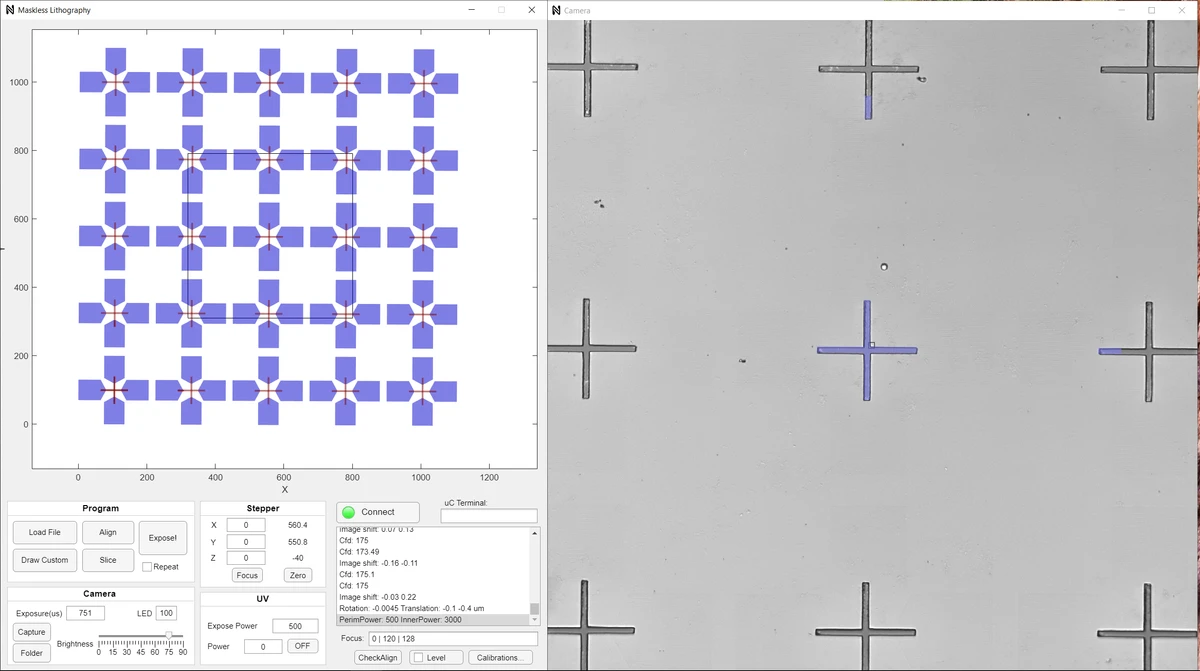
BeamXplorer control software — pattern layout view beside the live wafer camera with alignment marks
BeamXplorer
WORKFLOW

Less time in cleanroom.

BeamXplorer was designed to be intuitive. WASD navigation. Right-click anywhere to get there.

  • 01Auto image-recognition aligns multilayer jobs in minutes
  • 02Batch-queue exposures and walk away — abort-safe job queue
  • 03Inspect, focus-profile and wafer-map without leaving the tool
  • 04Develop greyscale dose like a photo — for true 3D microstructuring
DESIGN

Draw masks in your browser.

Glyph is BEAM's companion design tool — a free GDSII mask editor that runs entirely in your browser. No install, no upload; your designs stay on your machine.

  • 01AI-assisted drawing — prompt Claude to draft your layout, with one undo step per prompt so you can iterate safely
  • 02Bring sketches, photos, or microscope captures straight in. Trace Bitmap converts them into editable GDS polygons
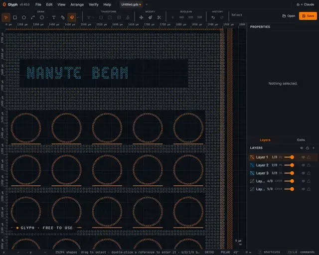
  • 03Modern direct manipulation — alignment guides, dynamic-input HUD, AutoCAD-style precision drafting
Start using Glyph
MISSION

Advanced lithography
for more labs.

01 / The Platform

NANYTE builds compact maskless lithography tools for labs that need serious patterning capability without the footprint, cost, or complexity of legacy systems.

02 / The Build

Behind BEAM is a small team of engineers and scientists who built every component from the ground up — optics, controllers, software. Making lithography this compact wasn't about shrinking what existed; it required redesigning what's inside.
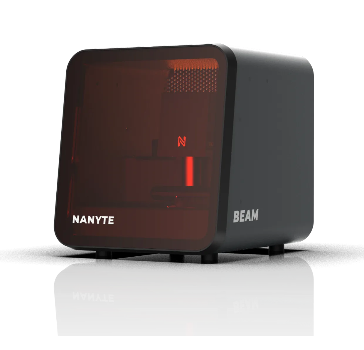

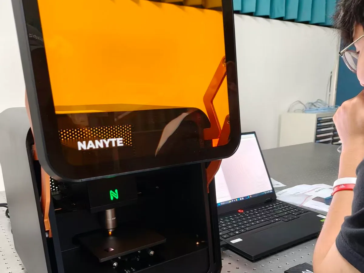
NANYTE BEAM benchtop maskless lithography system — product render with UV-protective viewport
40+ INSTITUTIONS WORLDWIDE · TRUSTED IN THE CLEANROOM
Nanyang Technological University
National Taiwan University
National Taiwan Normal University
Singapore University of Technology and Design
Agency for Science, Technology and Research
University of Birmingham
NC State University
Lanzhou University
TH Wildau
Linfield University
TSMC
Universidad Autónoma de Madrid
Available through · Distribution Partners

BEAM is designed and manufactured by NANYTE (Singapore). The same system is also offered as POLOS® BEAM through Semiconductor Production Systems (SPS) and distributed by SIMTRUM — all the identical NANYTE-built tool.

News

Latest from NANYTE.

All news →
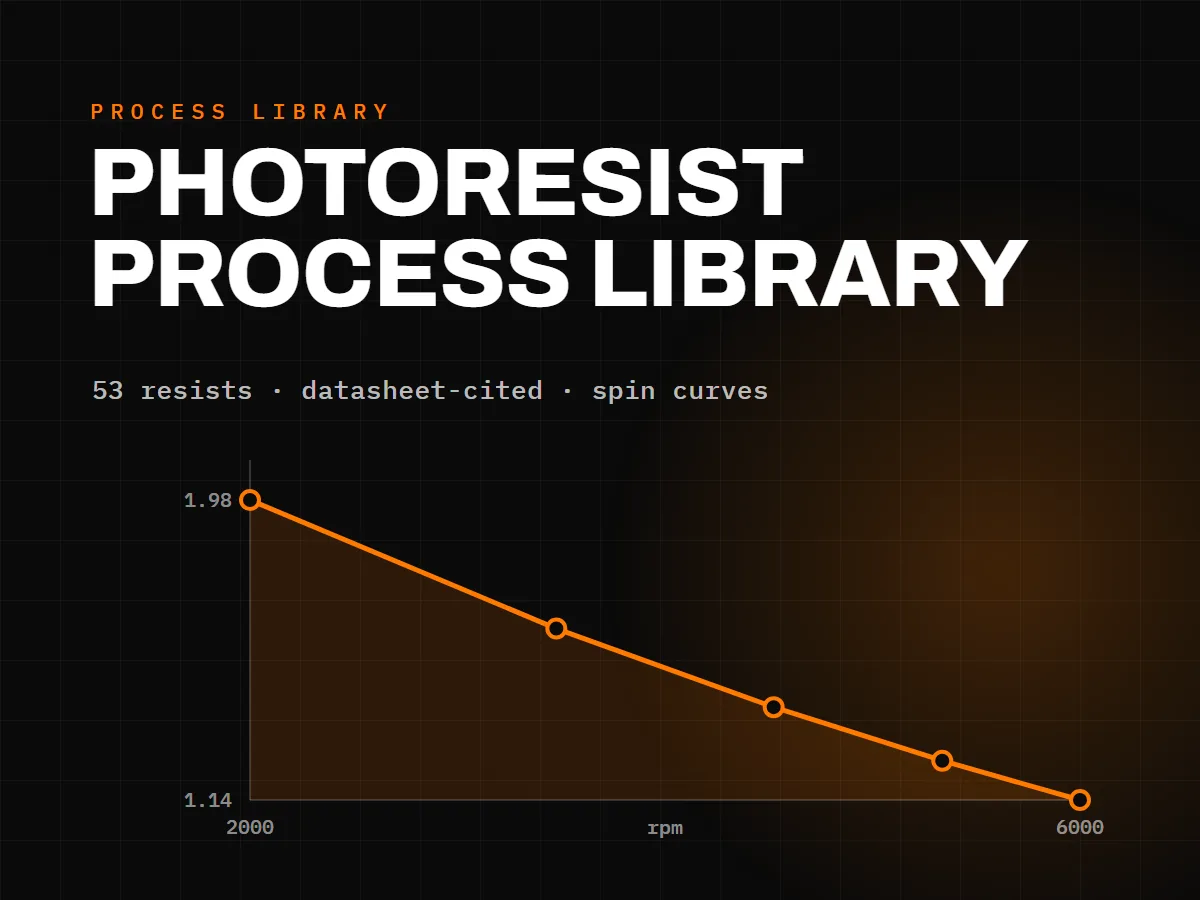
A dark card titled Photoresist Process Library showing an orange AZ 5214E film-thickness spin curve descending from 1.98 to 1.14 micrometres across 2000 to 6000 rpm
Company

A free photoresist process library.

NANYTE has published a free process library of 53 photoresists — datasheet-cited spin curves, bake and develop steps, tone and thickness filters, and a machine-readable copy of the whole dataset. No account, no registration.

PROCESS LIBRARY

Spin curves, bake schedules and doses for 53 common photoresists.

Every value cited to the manufacturer's datasheet — free, no login.

Browse the recipe library →
BEAM · maskless lithography FAQ

Frequently asked.

The NANYTE BEAM is a desktop (benchtop) maskless lithography system — a UV direct-write tool that patterns wafers and substrates directly from a digital layout, with no photomask. It reaches sub-0.4 µm resolution across a full 8-inch (200 mm) wafer, in a footprint that sits on a lab bench.

How maskless lithography works →

BEAM reaches a minimum feature size of 0.4 µm and a guaranteed 0.5 µm pitch, held edge to edge across a full 8-inch (200 mm) wafer — with 0.5 µm through-the-lens overlay and 0.1 µm bidirectional stage repeatability. To help you reach optimal linewidths, NANYTE also supplies process guidelines for common photoresists.

Browse the photoresist recipe library →

BEAM's Advanced engine exposes in 16-bit grayscale — 65,536 dose levels — so it can write smooth 3D and variable-depth structures such as micro-optics, blazed gratings, microlens arrays, and grayscale reliefs in a single exposure, rather than stacking binary layers.

BEAM's Advanced optics engine is optimized for 405 nm (h-line), with 365 nm (i-line) software-selectable. 405 nm gives the best transmission through the optics and works with most thin positive photoresists — for example Microposit S1805, AZ 5214E, and AZ ECI 3007. 365 nm covers i-line-sensitive resists that respond weakly or not at all at 405 nm, such as AZ nLOF lift-off resists and the SU-8 family — so one tool spans both with no hardware change.

BEAM is used across photonics, MEMS, microfluidics, micro-optics, metamaterials, grayscale lithography, rapid prototyping, and general research patterning — anywhere mask sets are too slow or too expensive. It is in use at 40+ universities, fabs, and R&D labs worldwide.

BEAM patterns on Si, SiC, GaN, single-crystal diamond, glass, sapphire, III-V (GaAs/InP), MEMS wafers, and — with limits — flexible substrates, at sample thicknesses from 0 to 7 mm, on a non-vacuum chuck as standard (vacuum optional). Sample sizes run to 130 × 130 mm on the BEAM stage, 6-inch (150 mm) on BEAM XL, and 8-inch (200 mm) on BEAM XL8. The TTL autofocus works through the projection path and is transparent-substrate compatible, so glass and sapphire focus directly. Layouts import as GDSII, OASIS, CIF, DXF, Gerber, BMP, PNG, TIFF, or JPG, or can be drawn in-software — Glyph, NANYTE's free browser-based GDS editor at nanyte.com/glyph, is the design companion.

BEAM can expose one writefield in under 0.1 s, depending on the resist's dose requirements — a very high power-density UV LED delivers the intensity to clear most resists in a single short flash. Overall throughput then depends on the objective: from about 3 mm² per minute at 50× (0.5 µm pitch) up to 500 mm² per minute at 2.5×, letting you trade resolution for write speed on each job.

BEAM is designed to run without cleanroom-scale infrastructure: the tool installs on a standard lab bench and runs from a wall socket — 110/230 V AC at under 50 W, with no compressed air, gas, or cooling water, vibration isolation built in, and a safety interlock that stops exposure when the door opens. The practical cleanliness requirement comes from your resist process (spin-coating and development), not from the tool itself, and NANYTE supplies process guidelines for common photoresists.

Photoresist processing guidelines →

We know of no other maskless lithography system that reaches 0.4 µm at BEAM's price point — submicron writing at a fraction of the price of established systems. Every BEAM is quoted individually, so there is no fixed list price: cost depends on the stage (BEAM, XL, or XL8) and the optics engine (Lite, Standard, or Advanced) you choose. Request a quote and NANYTE responds within 1–2 business days.

It depends on the configuration, so BEAM is quoted per system rather than at a fixed list price — the main cost factors are the stage you choose, the optics engine and its objective set, and any options. Just as important is the total cost of ownership: because BEAM is a true desktop tool that installs in minutes and runs from an ordinary wall socket — no compressed air, gas, cooling water, or cleanroom-scale infrastructure — it avoids the facilities and installation costs that larger direct-write systems carry. Tell NANYTE your application and we'll put together a quote and, where possible, a demo, with a reply within 1–2 business days.

Labs typically shortlist BEAM alongside established direct-write laser writers such as the Heidelberg Instruments µMLA/DWL series and the Durham Magneto Optics MicroWriter, and as a maskless alternative to a contact mask aligner. What sets BEAM apart: it is a true desktop tool — from 310 × 340 × 335 mm and 20 kg — that runs from a wall socket with no compressed air, gas, or water; it writes sub-0.4 µm features with 0.5 µm through-the-lens overlay across a full 8-inch wafer; the Advanced engine adds 16-bit grayscale and software-selectable 365 + 405 nm; and the stage and optics engine are specified independently, with the engine field-upgradeable later. We know of no other maskless system that offers 0.4 µm at BEAM's price point. Request the datasheet to compare specifications line by line against your current quotes.

Yes. NANYTE (NANYTE Pte. Ltd., Singapore) designs and manufactures BEAM and is the OEM. The same system is sold through distribution partners under their own branding — including as POLOS® BEAM through Semiconductor Production Systems (SPS) and via SIMTRUM — so 'POLOS BEAM' and Simtrum's BEAM are the identical NANYTE-built tool, with the same specifications. It is sometimes searched as a direct-write or 'laser writer' system; BEAM is a UV-LED/DMD maskless tool. For demos and the full datasheet, contact NANYTE directly at [email protected].

Email [email protected] or use the enquiry form on this page. Depending on your location, NANYTE can arrange an online demo or a live, in-person one, and will share the full specification datasheet on request. Expect a reply within 1–2 business days.

Have a question that isn’t answered here?

CONTACT

Talk to an engineer.

If BEAM looks like a tool you need, we'll arrange a demo — in your cleanroom or ours.

ADDRESS126 Joo Seng Rd, #08-05
Singapore 368355
HOURSMon – Fri · 09:00 – 18:00 SGT
Enquiries go straight to NANYTE.
ENQUIRY