Why photomasks exist — and what they cost
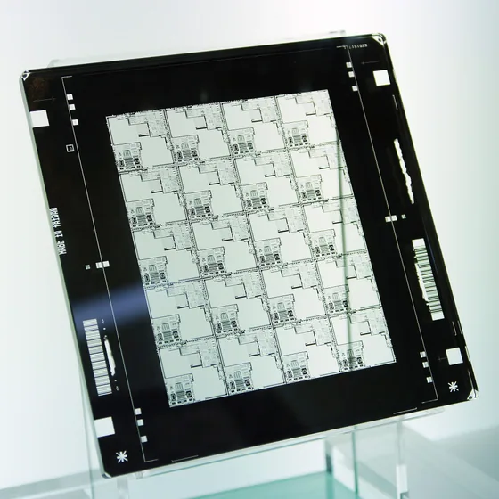
Conventional photolithography prints a pattern the way a darkroom prints a photograph: UV light floods through a photomask — a chrome-patterned glass plate — and transfers the entire design onto a resist-coated substrate in one flash. It is fast, repeatable, and utterly proven; it is how every chip in your pocket was made.
The catch is the mask itself. Every design revision needs a new plate, fabricated by a specialist vendor, at meaningful cost and days-to-weeks of lead time. In volume production that cost amortizes over thousands of wafers and disappears. In research it inverts: a device that will be redesigned five times pays for five masks and waits five times. Iteration — the core activity of R&D — becomes the slowest and most expensive step in the loop.
To be clear: for high-volume manufacturing of a frozen design, mask-based exposure still wins on throughput. Maskless lithography exists for everything before that point — and for structures a binary mask cannot make at all, like grayscale relief.
How maskless systems write a pattern
Every maskless tool replaces the photomask with something programmable. Three families dominate:
- UV laser — a single focused beam
- Fixed fold mirror
- Rotating galvo mirror — sweeps the beam
- Objective — focuses the spot into the resist
- Resist on the substrate: written point by point, one spot at a time
- UV LED — floods the whole array
- DMD — each micromirror switched on (orange) or off
- Projection optics — image the frame onto the resist
- Resist on the substrate: one whole writefield per flash, in parallel
- The stage steps to the next field
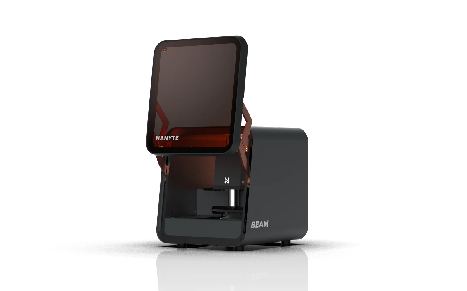
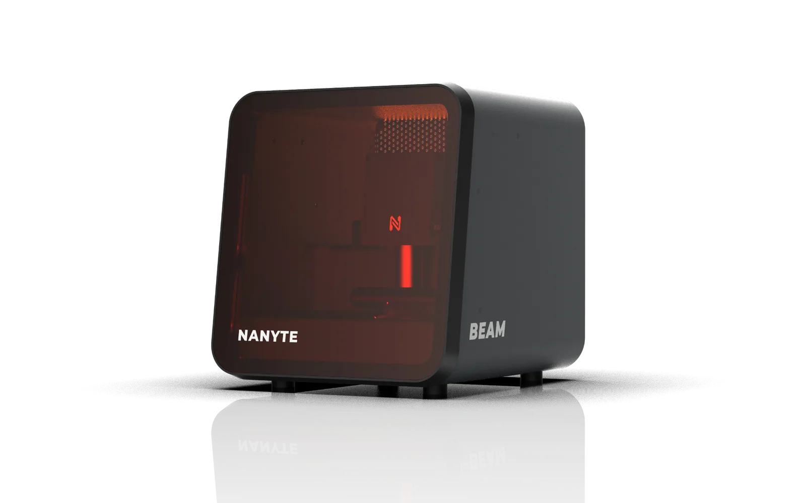
NANYTE has shipped both architectures: BEAM Gen 1 scanned a focused UV laser through a rotating galvo mirror; the Gen 2 engine replaced the scanned spot with a DMD that exposes a full writefield per flash.
DMD projection (digital micromirror device)
An array of millions of individually switchable micromirrors forms a dynamic mask. The optics project the mirror image onto the resist, exposing an entire writefield in one flash; the stage then steps to the next field and the software stitches fields into one seamless pattern. This is the architecture of the NANYTE BEAM and of most modern UV maskless aligners.
Laser direct write
A focused laser spot scans the design serially, like a plotter. Resolution is set by the spot size; write time scales with the patterned area. Laser writers are the traditional tool for fabricating photomasks themselves — a maskless tool that makes masks for everyone else.
Electron-beam lithography
A focused electron beam writes with nanometre-scale resolution — the highest of any maskless technique — but serially, under vacuum, at correspondingly low throughput and high cost. E-beam owns the regime below what UV optics can resolve.
From layout to patterned resist
- Import the layout — GDSII, OASIS, CIF, DXF, DWG, SVG, Gerber, or a plain bitmap.
- The software prepares the design for exposure, writefield by writefield.
- The tool exposes field by field, autofocusing and aligning as it steps.
- Develop the resist — the pattern is ready for etch, lift-off, or plating.
Where the mask file comes from
Every step above assumes the pattern already exists as a file. Going maskless removes the chrome-on-glass plate, not the layout work behind it: the tool still needs a mask file, with the geometry sorted onto numbered layers, before it can expose anything. Layouts come out of the usual EDA and CAD flows — but a lot of what a lab actually writes, from alignment marks and test structures to electrode arrays and channel networks, is smaller than a full EDA seat is built for.
Glyph is NANYTE’s answer to that: a free GDSII mask editor that runs in the browser. There is nothing to install and no account to create, and the reading, editing and writing all happen inside the page — your design never leaves your machine.
What it opens, and what it writes
Glyph opens GDSII, OASIS, DXF (ASCII and binary), DWG, CIF and SVG, plus PNG and JPG images to trace over and TTF/OTF fonts for labelling. It writes GDSII, OASIS, DXF, CIF, SVG, EPS and PNG. Three of those are one-way and worth knowing before you rely on them: DWG is read-only, and PNG and EPS are rendered output — figures for a paper or a slide, not layout you can open again.
Handing the design to the tool
With BeamXplorer running on the same computer and the link enabled, Glyph hands the design over and prepares the job — nothing goes over the internet, and Glyph never starts an exposure; the operator does that at the tool.
Glyph is free to use — open the editor at nanyte.com/glyph/. It is a general-purpose mask editor, not a BEAM front end: the files it writes go to any tool that reads the format.
How does DMD projection work?
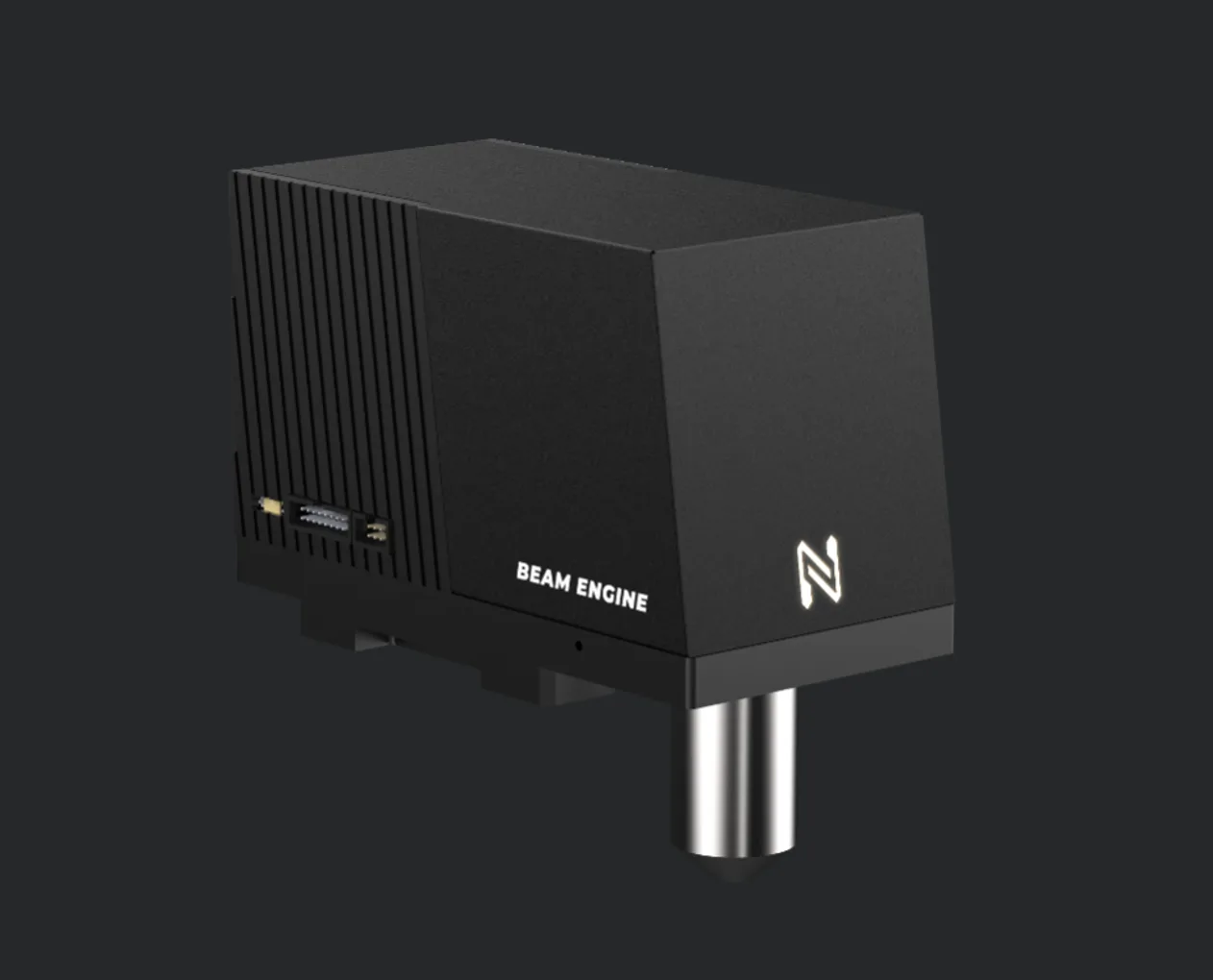
A digital micromirror device is a chip carrying millions of aluminium micromirrors, each a few microns across, each electrostatically tilted to either reflect UV light into the projection path (“on”) or dump it into an absorber (“off”). Loaded with a frame of the design, the array becomes a photomask that can change completely every few milliseconds — 1920 × 1080 mirrors on typical engines, 3K on high-end ones.
The projection optics demagnify the mirror image onto the substrate, so one frame exposes one writefield. With a high-power UV LED behind the DMD, a single flash can clear most resists — on the NANYTE BEAM, a writefield exposes in under 0.1 s, depending on the resist’s dose requirements. The motion stage steps between fields, and features that cross field boundaries print seamlessly across a full wafer.
Why wavelength matters
Resists, not tools, dictate wavelength. At 405 nm (h-line) most thin positive resists — Microposit S1805, AZ 5214E, AZ ECI 3007 — expose efficiently. At 365 nm (i-line) the resists that barely respond at 405 nm become available: AZ nLOF lift-off resists and the SU-8 family that microfluidics runs on. Dual-wavelength engines such as BEAM’s Advanced switch between the two in software, so one tool spans both resist classes with no hardware change. Spin curves, bake schedules and development parameters for these resists are collected in our photoresist process recipe library.
What sets the resolution
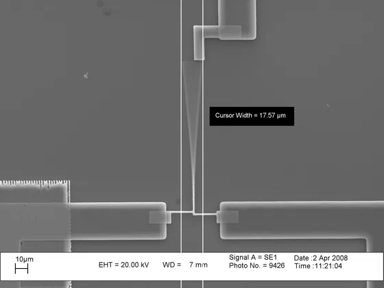
Resolution is diffraction-limited by the numerical aperture of the projection objective. Swapping objectives therefore trades resolution against field size and write speed: on BEAM’s demonstrated objective ladder, a 50× objective writes <0.5 µm features at 3 mm²/min while a 2.5× objective covers 500 mm²/min at 6.0 µm — the same engine, re-tasked in seconds. Large-NA optics with matched compensation hold that resolution edge-to-edge: BEAM writes sub-0.4 µm features across a full 8-inch (200 mm) wafer.
Figures quoted for BEAM are demonstrated performance; guaranteed specifications are in the full spec tables.
What is grayscale lithography?
Because every DMD pixel’s dose is individually controllable, exposure needn’t be binary. Modulating the dose per pixel exposes the resist to a controlled partial depth; after development, what remains is a three-dimensional relief — written in a single exposure, where a mask-based flow would stack and align many binary layers to approximate the same shape in staircase steps.
Bit depth decides how smooth that relief can be. An 8-bit engine has 256 dose levels; a 16-bit engine has 65,536 — the difference between visibly stepped and optically smooth surfaces. That is what makes grayscale exposure practical for micro-optics: microlens arrays, blazed gratings, diffractive elements, and variable-depth fluidic structures. See grayscale structures patterned with BEAM in the sample gallery.
Maskless vs photomask vs e-beam
There is no universally best patterning technique — there is a best technique per phase of work. The table compares the four options a lab typically weighs:
| Technique | Contact aligner | DMD maskless | Laser writer | E-beam |
|---|---|---|---|---|
| Typical resolution | ~1 µm | 0.3–1 µm | 0.3–1 µm | ~10 nm |
| Photomask required | Yes — one per revision | No | No | No |
| Cost per design change | New mask each time | None — digital | None — digital | None — digital |
| Equipment cost | $ | $$ | $$$$ | $$$$$ |
| Iteration turnaround | Days–weeks (mask fab) | Minutes | Minutes–hours | Hours (vacuum, serial) |
| Exposure mode | Full-field flash | Writefield flash + stitch | Scanned spot | Scanned beam |
| Grayscale / 3D | No | Yes — dose per pixel | Some tools | Yes (slow) |
| Best for | Volume runs of a frozen design | R&D, prototyping, grayscale | Photomask making, R&D | Nanoscale research |
Category-level, indicative figures — individual tools differ. For BEAM’s specific numbers, see the full specifications. Weighing specific benchtop systems against each other? See BEAM vs benchtop laser writers.
What maskless lithography is used for
Microfluidics
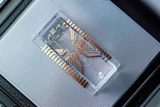
Channel networks and master molds, typically in SU-8, where geometry is the experiment: chip designs iterate daily instead of waiting on mask deliveries, and tall, high-aspect-ratio structures come from thick-resist exposure at 365 nm.
MEMS
Released mechanical structures need multiple aligned layers. Digital, through-the-lens overlay alignment lets prototype MEMS runs proceed without buying a mask set per layer per revision.
Photonics & micro-optics
Waveguides, ring resonators, and gratings at submicron linewidths — and, with grayscale exposure, blazed and diffractive profiles written directly rather than approximated in binary steps.
2D materials & quantum devices
Contacts and Hall-bar geometries drawn around individual, irregularly placed flakes — a use case a fixed mask fundamentally cannot serve, because every exfoliated flake lands somewhere new.
Rapid prototyping & teaching
One benchtop tool covering the whole design-expose-develop loop makes lithography accessible outside billion-dollar fabs. Maskless tools now run in university cleanrooms and R&D labs worldwide — BEAM alone is in use at 40+ institutions. Browse structures patterned with BEAM.
Where maskless lithography stops
Three boundaries are worth knowing before you buy anything. First, volume: once a design is frozen and wafer counts climb, a photomask’s one-flash-per-design economics beat any maskless tool — production lines will keep buying masks. Second, feature size: UV optical maskless is diffraction-limited, so features well below ~0.2 µm belong to e-beam or DUV/EUV steppers. Third, time: writing a full wafer at maximum resolution takes correspondingly longer than flashing it through a mask — maskless throughput is engineered for iteration, not replication.
Choosing well means matching the tool to the phase of work: maskless for everything that changes, masks for everything that doesn’t.
Maskless lithography FAQ
Product-specific questions — pricing, configurations, comparisons with other systems — are covered in the BEAM FAQ.